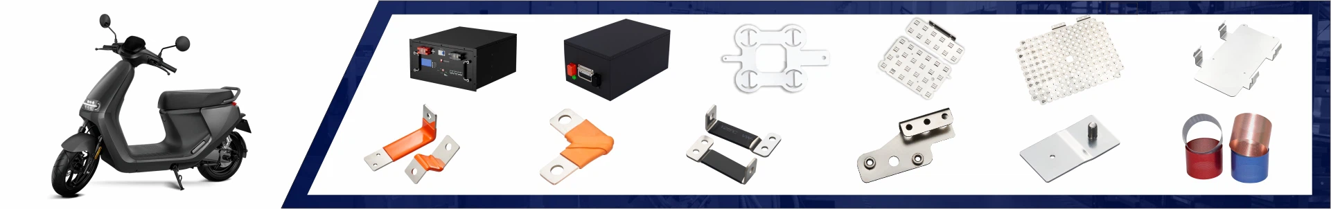


Stamping Processing Copper Nickel Sheet
●Product name:Battery connector copper nickel sheet
●Material:Copper sheet + nickel sheet
●Nickel Purity:99.5%
●Copper Purity:72%
●Application:battery pack, industry
●Type:Nickel Strip
●Size:Customized
●Delivery Time:7~20 DAYS


Custom Stamping Processing for Copper-Nickel Composite Sheets
Custom Stamping Service for Copper-Nickel Composite Sheets - Precision Bimetal Component Manufacturing
We provide specialized stamping processing services for copper-nickel composite sheets, creating precision components that leverage the unique properties of both metals. Our advanced stamping technologies transform bimetal materials into functional parts with electrical, thermal, and mechanical advantages. This service is ideal for applications requiring controlled current distribution, thermal management, or corrosion resistance in specific areas. From battery terminals to power connectors, we deliver custom-stamped components that meet exacting specifications for demanding electrical and electronic applications.
|
Product name |
Custom layered copper-nickel sheets |
|
Material |
70/30, 80/20, 90/10 Cu-Ni) |
|
Material Thickness |
0.3mm - 4.0mm total thickness (individual layers 0.1mm - 2.0mm) |
|
Stamping Precision |
±0.02mm critical dimensions, ±0.05mm general features |
|
Size |
0.15mm hole diameter, 0.2mm slot width |
|
Layer Alignment Control |
±0.05mm layer registration accuracy |
|
Production Method |
Progressive die stamping, compound die stamping, transfer press operations |
|
Secondary Operations |
Heat treatment, stress relieving, selective plating, laser trimming |
|
Quality Standards |
Dimensional tolerance per ISO |
Product Features
▲Bimetal Interface Integrity
Specialized tooling designs maintain perfect alignment between copper and nickel layers throughout stamping operations, preventing delamination or interface damage.
▲Selective Property Engineering
Strategic material placement allows different functional areas to exhibit copper's conductivity or nickel's durability within a single stamped component.
▲Edge Quality Preservation
Proprietary stamping techniques produce clean, burr-free edges that maintain both metals' integrity without requiring extensive secondary finishing.
▲Stress Distribution Optimization
Tooling designs specifically account for different material behaviors in bimetal sheets, minimizing residual stresses and ensuring dimensional stability.
▲Thermal Management Integration
Component designs incorporate thermal expansion considerations for both materials, ensuring reliable performance across temperature cycles.
▲Controlled Layer Exposure
Precision stamping creates selective exposure of desired metal layers at specific contact points without secondary machining operations.
▲High-Volume Consistency
Automated stamping processes ensure identical bimetal alignment and dimensional accuracy across large production runs.


Product Applications
▲Electromobility Components: Battery cell connectors, power distribution bars, charging interface components
▲Power Distribution Systems: Busbar segments, circuit breaker contacts, switchgear components
▲Renewable Energy Systems: Solar panel connectors, wind turbine slip ring contacts, inverter components
▲Telecommunications: RF shielding components, waveguide flanges, antenna contacts
▲Medical Electronics: Diagnostic equipment contacts, surgical instrument components, imaging system parts
▲Industrial Sensors: Temperature sensor components, current sensing shunts, transducer elements

Customization Workflow
▲1: Material Configuration Design
Collaborative design of optimal copper-nickel layer ratios, thicknesses, and arrangements based on electrical, thermal, and mechanical requirements.
▲2: Stamping Process Simulation
Advanced finite element analysis simulates stamping behavior to predict material flow, stress distribution, and potential delamination risks.
▲3: Progressive Die Engineering
Design and fabrication of specialized progressive dies with features to accommodate bimetal characteristics and ensure proper layer handling.
▲4: Process Parameter Optimization
Establishment of precise stamping parameters including pressure, speed, and lubrication specifically calibrated for copper-nickel composites.
▲5: Prototype Validation Series
Production of prototype batches for functional testing including electrical continuity, thermal cycling, and mechanical stress evaluation.
▲6: Production Ramp-up & Quality Verification
Graduated production scaling with comprehensive quality verification at each stage, ensuring process stability before full-volume manufacturing.


FAQ
Q1: What are the primary advantages of using copper-nickel composites over single-metal stamped parts?
Copper-nickel composites combine the excellent electrical conductivity of copper with the superior corrosion resistance and durability of nickel. This allows specific areas of a component to be optimized for different functions-contact points can be nickel-rich for durability while current paths remain copper-rich for maximum conductivity.
Q2: How do you ensure the copper and nickel layers remain properly bonded during stamping operations?
We employ specially designed tooling with controlled pressure gradients and use proprietary stamping sequences that maintain compression at the material interface. Our processes are validated through cross-sectional analysis and peel testing to confirm bond integrity throughout deformation.
Q3: Can you produce parts with different copper-nickel ratios on different areas of the same component?
Yes, we utilize specialized material preparation techniques that allow varying layer ratios across different regions of the sheet before stamping. This enables components with, for example, nickel-rich contact areas and copper-rich current paths within a single stamped part.
Q4: What design considerations are unique to copper-nickel composite stamping that differ from single-metal stamping?
Key considerations include differential spring-back between materials, thermal expansion management, galvanic corrosion prevention at exposed edges, and tooling designs that accommodate different material flow characteristics. Our engineers work closely with clients to optimize designs for successful bimetal stamping.
Hot Tags: stamping processing copper nickel sheet, China stamping processing copper nickel sheet manufacturers, suppliers, factory, 18650 Copper Nickel Sheet, Battery Copper nickel Sheet, Welding Battery Pack Copper Nickel Sheet


Send Inquiry